
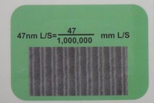
If you need to make 47nm lines and spaces, we’ve got the hardware you need:
https://www.fabsurplus.com/sdi_catalog/salesItemDetails.do?id=89012
With a 193nm immersion scanner, developed by Nikon, the world’s first to break the barrier for an NA of 1.0 reaching an NA of 1.07, enabling the mass production of devices with a resolution of 55nm.
Immersion Lithography technology allowed a step forward in resolution in the semiconductor industry. The challenge of this technology is how to deal with a purified medium (like water or oil) filling the space between the projection lens and the substrate.
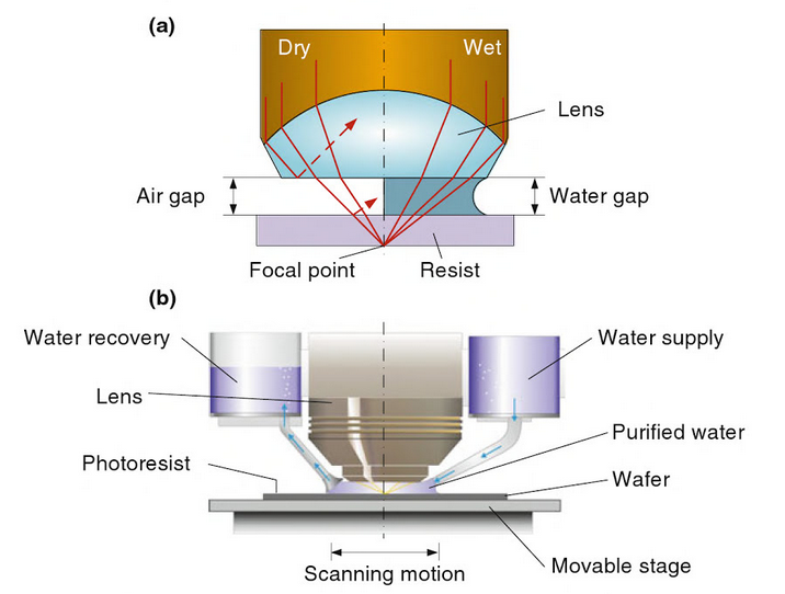
(a): Air gap and water-filled gap between lens and substrate. Liquid between objective lens and image plane reduces the angle of the light exiting the lens
(b): Immersion lithography lens/wafer arrangement
(source: Micro and Nano Fabrication: Tools and Processes, by Hans H. Gatzen,Volker Saile,Jürg Leuthold)