Semiconductor Process

Semiconductor Manufacturing Process Explained

Ever wondered what is the semiconductor manufacturing process?

What are the steps involved and what are the machines required?

Here’s an explanation!

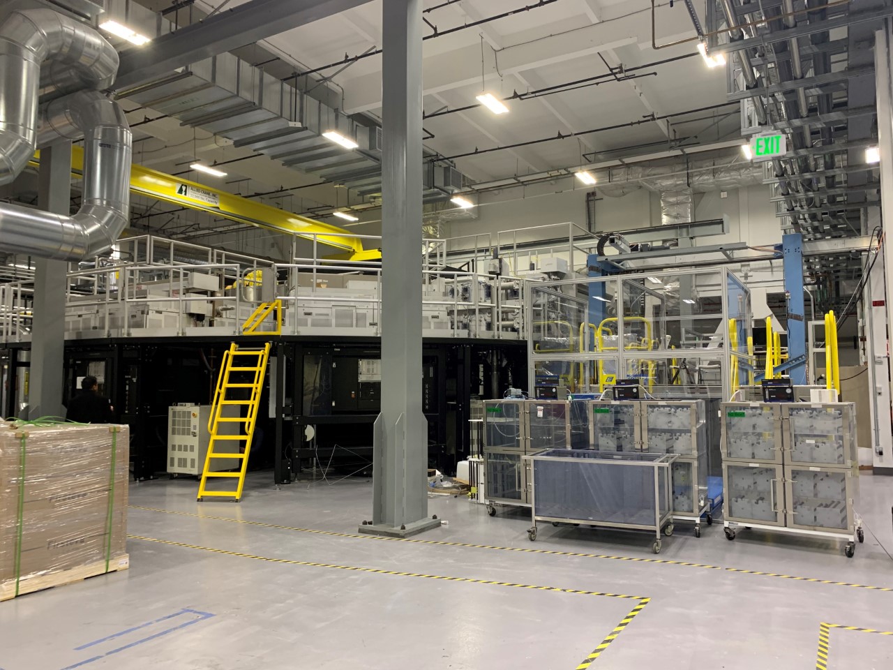
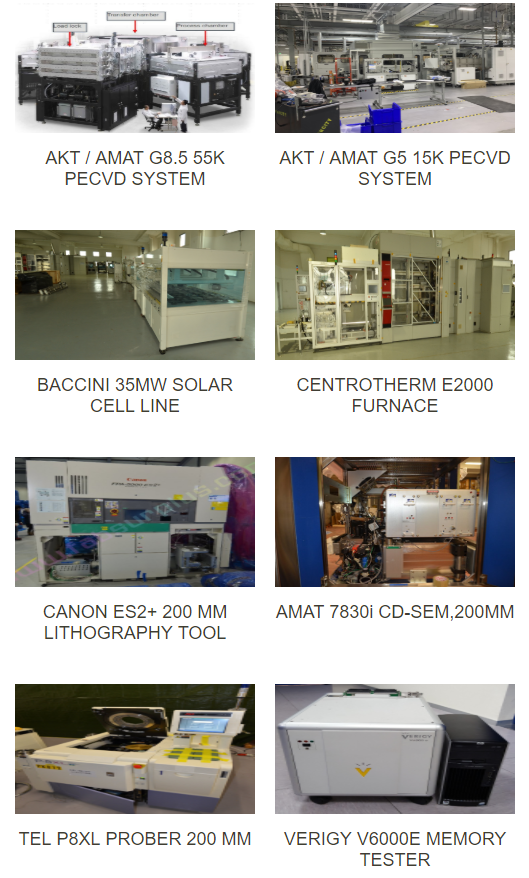
The Semiconductor production process consists of the Front End, in which circuits are placed on silicon wafers, and the Back End, which involves assembly and packaging. SDI Fabsurplus.com equipment for sale covers all aspects of this process.

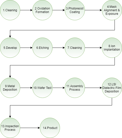
Points 1 to 10 of the Workflow below belong to the Front End semiconductor process.

Semiconductor manufacturing process flow


Let’s go into detail into most of the processes outlined above.

Oxidation formation

Wafers are placed into a rapid thermal processing system and heated to approximately 1000° Celsius. By exposing wafers to a flow of gas, various films , the oxidation, are created on the wafer surface.

View Rapid Thermal Processing Systems for sale

Photoresist Coating

While the wafers are rotated at a high speed in a coater, they are covered by a uniform coat of photoresist. The resist characteristics change when exposed to ultraviolet light thus, placing an image on the wafer.

View Coaters/Developers for sale

Mask Alignment Exposure

After glass masks with integrated circuit (IC) patterns are aligned with the wafers, ultraviolet (UV) liht is applied to transfer the patterns to the photoresist using a stepper.

View Steppers, Scanners and Photolithography Equipment for sale

Develop

In a developer, the wafers are uniformly covered with a developing solution to develop the mask patterns. With positive photoresist, the portion that has been exposed to light becomes soluble, leaving the mask patterns on the wafer surfaces.

View Coaters/Developers for sale

Etching

A plasma dry etch system is used to strip the dielectric films in accordance with the patterns developed on the photoresist. The portion protected by the photoresist remains intact, preserving the original film structure under the resist

View Dry Etch equipment for sale

Ion Implantation

Ion implantation dopes or implants the surface of the wafer with a known quantity of impurities, such as boron and arsenic. These elements are then shot into the wafer in a bullet-like fashion. Sacrificial films exist, preventing ions from being implanted in unwanted areas of the wafer. Subsequent annealing will diffuse these impurities to a more uniform density.

View Ion implanters for sale

Interconnect Dielectric Film Deposition

Films are deposited to insulate the devices (transistors) and wires. The deposition technique may use a CVD (Chemical Vapor Deposition) system that accumulates gaseous materials through chemical reactions or an SOD (Spin-on Dielectric) coater that applies liquid material through spinning.

View Photoresist Coat and Development equipment for sale

Metal Deposision / Etching

After the inter-layer dielectric (ILD) films are etched, a CVD (Chemical Vapor Deposition) or PVD (Physical Vapor Deposition) system is used to deposit metal films to form wiring.

View PVD equipment for sale
View CVD equipment for sale

Wafer Test

Each completed wafer contains hundred of identical ICs. A wafer prober and a tester work together to inspect these individual ICs . Results of these tests determine “good” and “bad” ICs.

View Wafer probers for sale

View Testers for sale

Assembly Process : Dicing

Following wafer test, the ICs on the wafer are cut into IC chips several square-millimeters in size utilizing either a diamond cutter or laser technology.

View Dicing Saws for sale

Assembly Process: Bonding / Completed LSI

Each IC chip pads and package terminals are connected via metal wiring and the chip is enclosed in the appropriate packaging (e.g. plastic). The LSI manufacturing process is now complete.

View Assembly Bonders for sale

Hope you have enjoyed this introduction to the semiconductor manufacturing process, brought to you by SDI Fabsurpus.com. Are you looking for used semiconductor manufacturing equipment for sale?

Look at our website: www.fabsurplus.com


Final reminder! Large-Format Flat Panel Display – Solar Cell, Semiconductor Reliability and Wafer-Fab Equipment Short Notice Clearance Sale

Featuring Excellent Recent-Vintage G8.5 and G5 Amorphous Silicon PECVD Deposition Systems with Many Other Semiconductor and Solar-related Equipments.

Under the Instruction of a Leading US-based Manufacturer of Solar Panels, we are pleased to offer the following high quality Solar Cell Testing, Large-format Solar Panel Manufacturing, Solar Cell Manufacturing, Semiconductor Test, Reliability and Semiconductor Wafer Fab Equipment for immediate sale via closed-bid.
Major items include:
  • An AKT / Applied Materials G8.5 55K Amorphous Silicon PECVD Deposition System.
  • An AKT / Applied Materials G5 15K Amorphous Silicon PECVD Deposition System.
  • A Jonas and Redmann CTS 3600 solar cell tester and sorter.
  • A Sheffield Endeavor Coordinate Measurement System.
  • A fully-automated 35 MW Baccini Solar Cell Production line.
  • A Centrotherm E2000 Phosphor Doping Furnace.
  • A Canon ES2+ 248 nm lithographic scanner for 200 mm wafers.
  • An ELES ART 200 Burn-in-Board testing system.
  • An Applied Materials 7830i CD-SEM for 200 mm wafers.
  • KLA-Tencor Surfscan AIT UV Fusion wafer inspection system for 200 mm wafers.
  • Two Mazzali Climatest C320G5 Temperature and Humidity Test Chambers.
  • A Roth and Rau SiNa Plus PECVD Silicon Nitride Deposition System for Solar Cells
  • A RENA Edge-Isolation System for Solar Cells.
  • An STS 320 PC Laboratory Reactive Ion Etcher for 200 mm wafers.
  • Two TEL MB2 730 HT WSi CVD deposition systems for 200 mm wafers.
  • An Agilent / Verigy V6000e Memory Tester.
  • A Weiss TS 130 Thermal Shock Testing Chamber.
  • Vacuum Pumps, 200 mm wafer bar-code readers, probers, chillers, testers, ovens, test handlers, oscilloscopes and much more !!

New lots include:

  • A Hitachi S9300 CD-SEM Scanning Electron Microscope, 200 mm.
  • Edwards PHMB2400 + PRV mechanical pumps qty 2.
  • Edwards iXH500H and iXH450H Mechanical Pumps.
  • Edwards iH1800 Mechanical Pumps qty 7.
  • Edwards iF30K Mechanical Pumps qty 3.
  • Edwards iXL5000Q Mechanical Pumps qty 3.
  • Edwards iXH3030 Mechanical Pumps qty 3.
  • Edwards Marathon S Exhaust Gas Scrubbers qty 3.
  • Daihen RGA-150A1 15 KW RF Generators, qty 4.
  • Edwards Neptune Exhaust Gas Scrubber.

Auction Closes 23rd of May.
Place your bid now !

A video of the AKT PECVD G8.5 55k Amorphous Silicon Deposition System is shown here:-
https://youtu.be/GP-AxxVEhbU

A video of the AKT PECVD G5 15k Amorphous Silicon Deposition System is shown here:-
https://youtu.be/gDHjfOPo7Pc

Auction Catalog

Here follows the list of lots available for purchase in this sale, also listed in the attached excel file, available also to download by clicking here.
To See photos and technical specifications regarding each of these lots for sale, please click on the links shown below. To place a bid, please compile the auction agreement, attached, with the SDI ID of each lot which you wish to purchase, and send it back to us scanned, in order to register your bid properly.

Viewing of assets

You are very welcome to come and view any of the assets by appointment.
Assets are located in Fremont,California,  Temple,Texas,  San Antonio,Texas,  Kuala Lumpur,Malaysia and Avezzano, Italy.
To arrange a viewing, please send a mail to: auction@fabsurplus.com.

How to submit a bid

All assets will be sold by “Closed bid”.Click here to download a copy of the bid submission form. PLEASE FULLY COMPLETE AND SIGN THE ATTACHED BID SUBMISSION FORM, THEN SCAN IT AND SEND IT VIA E-MAIL TO: auction@fabsurplus.com.

Closing date

All bids should be submitted before 12 Midday on Thursday, 23rd May, 2019, Pacific Standard Time. You will be notified of your winning bids within 48 hours of the closing date.

We look forward to getting your bids and inspection requests very soon.
Thanks so much for your kind attention. 

Yours sincerely,

Stephen

SDI Fabsurplus LLC
Stephen Howe
Company Owner
email: info@fabsurplus.com
Mobile:(USA) +1-830-388-1071 
Mobile:(Italy) +39-335-710-7756
Skype: stephencshowe
WWW.FABSURPLUS.COM
Linkedin: https://www.linkedin.com/company/sdi-fabsurplus
Twitter: https://twitter.com/fabsurplus
Facebook: www.facebook.com/fabsurplus